
Inorganic/Organic and Organic/Organic Interfaces: Structure and Charge Transport
Summary
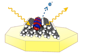
Interfaces between organic semiconductor (OSC) films and metallic electrodes or between different OSC-layers are of key importance for charge injection and exciton dissociation processes occurring in organic electronics. This project aims to prepare and characterize well-defined model interfaces with controlled molecular orientation and crystalline order to correlate their microstructure with the electronic and optical properties. The interfaces are prepared by organic molecular beam deposition and characterized by means of X-ray diffraction (XRD), atomic force microscopy (AFM), scanning tunneling microscopy (STM) and synchrotron-based photoelectron-spectroscopy (XPS, NEXAFS), and will be further used for complementary time resolved spectroscopy experiments and their theoretical modeling in other subprojects. Based on the results obtained in the first funding period we will continue to study the influence of molecular seed/primer layers on subsequent OSC-film growth as well as molecular acceptor/donor interfaces (including newly synthesized molecular materials) taking into account the following issues:
(1) To which extent is the molecular orientation in both systems artificially adjustable?
(2) Thermal stability of subsequently stacked layers, thermally activated intermixing? (comparison of intermixing in thick and metal substrate supported molecular layers)
(3) Chemical reactions at organic interfaces and adduct formation.
In addition, we will extend the class of substances also to 2D materials (TMDC (e.g. MoS2), h-BN). Here, we will address the topic of excitonic coupling between OSC films of various thickness and orientation and TMDC substrates, while h-BN films are used as spacer layers to study the electronic and excitonic coupling between two OSC layers.
Project-related publications of the principal investigator
- F. Widdascheck, A.A. Hauke, G. Witte
A Solvent‐Free Solution: Vacuum‐ Deposited Organic Monolayers Modify Work Functions of Noble Metal Electrodes
Adv. Funct. Mater. 29, 1808385 (2019). - D. Günder, K. Watanabe, T. Taniguchi, G. Witte
Van der Waals Bound Organic/2D Insulator Hybrid Structures: Epitaxial Growth of Acene Films on hBN(001) and the Influence of Surface Defects
ACS Appl. Mater. Interfaces 12, 38757 (2020). - M. Dreher, D. Günder, S. Zörb, G. Witte
Van der Waals Bound Organic Semiconductor/2D Material Hybrid Heterosystems: Intrinsic Epitaxial Alignment of Perfluoropentacene Films on Transition Metal Dichalcogenides
Chem. Mater. 32, 9034 (2020). - P.E. Hofmann, M.W. Tripp, D. Bischof, Y. Grell, A.L.C. Schiller, T. Breuer, S.I. Ivlev, G. Witte, U. Koert
Unilaterally Fluorinated Acenes: Synthesis and Solid-State Properties
Angew. Chem. Int. Ed. 59, 16501 (2020). - S.R. Kachel, P.M. Dombrowski, T. Breuer, J.M. Gottfried, G. Witte
Engineering of TMDC-OSC Hybrid Interfaces: The Thermodynamics of Unitary and Mixed Acene Monolayers on MoS2
Chemi. Sci. (accepted) DOI: 10.1039/d0sc05633b (2021).
Prof. Dr. Gregor WITTE
Daniel Bischof, PhD-student
Pierre Dombrowski, PhD-student
Maximilian Dreher, PhD-student
Darius Günder, PhD-student
Yurii Radiev, PhD-student
Former Contributors
Dr. Tobias Breuer, Researcher
Dr. Pablo Echeverry Enciso, Visitor
Dr. Alrun Hauke, Postdoc
Dr. Andrea Huttner
Dr. Michael Klues
Dr. Michael Kothe
Dr. Alexander Mänz
Dr. Felix Widdascheck