Unveiling the Effects of Hydroxyl-Induced Trap States on the Charge Transport in p- and n-Channel Organic Field-Effect Transistors through Variable-Temperature Characterization – Publication by A2
In a new publication in Advanced Materials, project A2 (Witte) reports on the variable-temperature transfer length method (TLM) investigation of p– and n-channel organic field-effect transistors (OFETs). The use of the developed full high vacuum (HV) process chain allows to exclude the effect of ambient exposure and reveals the effects of surface hydroxyl groups on the charge transport in OFETs.
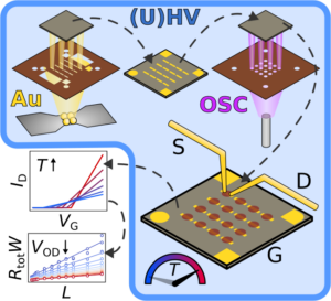
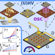
Schematic depiction of the full-vacuum process, clockwise from top left: patterning of the gold source-drain electrodes, patterning of the OSC active layer, variable-temperature electrical characterization, obtained transfer current-voltage characteristics and a resulting TLM plot.
Charge transport in organic semiconductors (OSC) is significantly affected by trap states, both intrinsic (due do dynamic disorder in molecular crystals) and extrinsic (occurring in devices at hetero-interfaces, due to chemical impurities, environmental exposure and bias stress). Especially in OFETs, where the conduction channel is formed in an immediate vicinity of the gate dielectric-OSC interface, the trap states at said interface might significantly affect the performance of the device. This is particularly relevant for devices with gate dielectrics based on inorganic oxides, such as silicon dioxide and alumina (Al2O3), where the dangling bonds at the surface are passivated by hydroxyl groups. For a long time it was considered that such surface hydroxyl groups form trap states that are relevant primarily for electrons, which made observation of n-channel conductivity in OFETs challenging. At the same time, multiple studies reported low effective mobilities of p-channel OFETs with hydroxylated dielectrics, however due to the belief established above this effect was mostly attributed to environmental exposure of prepared devices.
To unveil the actual effects of surface hydroxyl groups on the performance of both p– and n-channel conductivity, the authors develop a full-HV processing chain that allows to avoid exposure of OFETs to ambient air. Devices with a bare (hydroxylated) Al2O3 gate dielectric perform significantly worse than OFETs with a tetradecylphosphonic acid (TDPA)-functionalized dielectric, where the hydroxyl groups are replaced by TDPA molecules, regardless of the channel type. This is attributed to the hydroxyl-induced trap states at the gate dielectric-OSC interface. To allow a deeper understanding of the observed phenomenon, a variable-temperature TLM analysis is employed, which allows to extract the activation energy of the charge transport in the conduction channel and the injection barrier at the electrode-OSC interface. The results demonstrate that, unlike it is often assumed, the density of trap states at the gate dielectric-OSC interface plays a secondary role in the device performance. Instead, the activation energy and the injection barrier seem to define the latter. Furthermore, a strong correlation between the two quantities is observed. This indicates that the injection barrier is directly influenced by the efficiency of the charge transport in the conduction channel via the formation of a space charge region close to the injection interface.
The present study unveils the complex interplay between various performance parameters of OFETs, which allows to identify the limiting factors for the charge transport and opens possibilities for further improvements in the field of organic electronics.
See also press release by university of Marburg.
Publication
Y. Radiev, T. Wollandt, H. Klauk, G. Witte
Unveiling the Effects of Hydroxyl-Induced Trap States on the Charge Transport in p- and n-Channel Organic Field-Effect Transistors through Variable-Temperature Characterization
Adv. Mater. (2025) 2505631 DOI:10.1002/adma.202505631
Contact
Prof. Dr. Gregor Witte
Philipps-Universität Marburg
SFB 1083 project A2
Tel.: 06421 28-21384
EMAIL
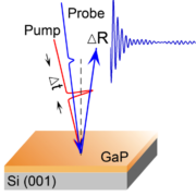
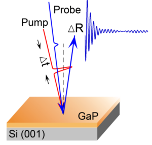 The key to their success was a new laser experiment that we started setting up in 2019. With intense excitation pulses, which are at the same time short enough for coherent phonon spectroscopy and widely tunable, Mette et al. could launch the phonons by resonantly exciting an electronic interface transition. The work has been conducted in collaboration with Kunie Ishioka from the National Institute for Materials Science (NIMS) in Tsukuba, Japan. The samples were grown and characterized by Wolfgang Stolz, former project A1, and Kerstin Volz, project A5, in Marburg.