
Novel single-atom sensitive imaging – Publication in Nature Materials by A12 (Tautz)
The team of researchers from Jülich, supported by SFB 1083 together with external partners, has developed a new method to measure the electric potentials of a sample with atomic accuracy. Using conventional methods, it was virtually impossible until now to quantitatively record the electric potentials that occur in the immediate vicinity of individual molecules or atoms. The new scanning quantum dot microscopy method, presented in the journal Nature Materials, also opens new ways of characterizing internal interfaces, as they often involve charge transfer and therefore show unique signatures in their electric potential.

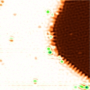
Image from a scanning tunnelling microscope (STM, left) and a scanning quantum dot microscope (SQDM, right). Using a scanning tunnelling microscope, the physical structure of a surface can be measured on the atomic level. Quantum dot microscopy can visualize the electric potentials on the surface at a similar level of detail – a perfect combination. (Copyright: FZ Jülich, Christian Wagner)
The positive atomic nuclei and negative electrons of which all matter consists, produce electric potential fields that superpose and compensate each other, even over very short distances. Conventional methods do not permit quantitative measurements of these microscopic fields, which are responsible for many material and interface properties and functions at the nanoscale. Almost all established methods capable of imaging such potentials are based on the measurement of forces that are caused by electric charges. Yet these forces are difficult to distinguish from other forces that occur on the nanoscale, which prevents quantitative measurements.
Four years ago, however, the scientists from Forschungszentrum Jülich discovered a method based on a completely different principle. Scanning quantum dot microscopy involves attaching a single organic molecule – the “quantum dot” – to the tip of an atomic force microscope. The molecule is so small that individual electrons from the tip of the atomic force microscope can be attached to the molecule in a controlled manner. With the new method it is not only possible to visualize the electric fields of individual atoms and molecules, it is also possible to quantify them precisely.
Finally, scanning quantum dot microscopy is particularly well-suited to study internal interfaces. This is illustrated, e.g., by its ability to clearly resolve sub-surface defects, as the team around Stefan Tautz has already demonstrated. For such investigations, the long-range nature of electrostatic potentials is an asset.
Publication
C. Wagner, M.F.B. Green, M. Maiworm, P. Leinen, T. Esat, N. Ferri, N. Friedrich, R. Findeisen, A. Tkatchenko, R. Temirov, and F.S. Tautz,
Quantitative imaging of electric surface potentials with single-atom sensitivity
Nature Materials (2019) DOI: 10.1038/s41563-019-0382-8
See also read-only access and German press release by FZ Jülich, as well as Nature Materials News & Views.
Contact
Prof. Dr. Stefan Tautz
Forschungszentrum Jülich
Peter Grünberg Institut
SFB 1083 project A12
Tel.: 02461 61 4561
EMAIL
 Jens Güdde, Univ. Marburg
 As the first half of SFB 1083’s second funding period comes to a close it was time for its principal investigators to get together to discuss in depth their individual project’s progress and how interdisciplinary research and discussion across projects are developing.